The rapid advancement of scientific research often leads to an overwhelming influx of data, particularly in experimental settings. Researchers at the U.S. Department of Energy’s Argonne National Laboratory have made significant strides in addressing this challenge by developing a novel computer chip designed to compress and process the vast quantities of data generated by advanced X-ray detectors. This innovation is particularly relevant for facilities such as the Advanced Photon Source (APS), a user facility of the DOE Office of Science located at Argonne.
The new chip works by compressing data directly at the source. This process can be likened to reducing the size of a digital movie or song, thereby facilitating easier transmission and analysis. By implementing this technology, experiments can be conducted more efficiently, allowing for quicker insights and more effective data management.
Advanced X-ray detectors function by capturing signals emitted when X-rays or electrons interact with a sample, similar to how a digital camera captures light to create photographs. These signals are transformed into electrical pulses and subsequently digitized into numerical data suitable for computer processing. However, the sheer volume of data produced by modern detectors can be staggering. Each frame, including those with minimal useful information, is transmitted for storage and analysis, which can overwhelm computational resources and hinder research progress.
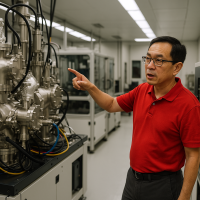
As physicist Antonino Miceli from Argonne and the University of Chicago articulates, “Our goal is to bring more computing right where the data is generated. In our earlier work, we demonstrated that advanced mathematical techniques could effectively reduce data volume while retaining critical information for analysis. Now, leveraging new chip technology and microelectronics advancements, we have developed a chip that incorporates this mathematical processing directly within the detector itself. Utilizing data from the APS 8-ID beamline, the detector can compress the data instantaneously as it is collected.”
This integration allows scientists to conduct essential calculations on the compressed data without the need for prior decompression. As a result, researchers can quickly analyse outcomes and receive feedback, even while ongoing experiments are still in progress.
Chips with Adaptive Learning Capabilities
Building upon their previous findings, the research team has integrated a compact, high-speed matrix-math processor directly into the detector chip. Rather than transmitting every pixel from the instrument, the chip synthesizes each image into a concise set of numbers that retains the most important features for scientific analysis. The output maintains a consistent size and streams in real time, facilitating improved data management.
To enhance the chip’s utility and adaptability, it can be customised for individual experiments. Prior to or during an experiment, scientists can input preset “weights”—configurations that instruct the chip on which features to prioritise. This process bears resemblance to training an artificial intelligence (AI) model. By using sample data, the chip can be tailored to focus on the most pertinent elements for each specific experiment. The findings from this research are documented in the Journal of Instrumentation.
As Argonne scientist Tao Zhou explains, “In essence, the chips can be trained on what is most important for the experiment, allowing them to compress and reduce data dynamically.” The hardware demonstrates flexibility and can be modified for various types of compression or data reduction, including radial integration. The Center for Nanoscale Materials (CNM), also a DOE Office of Science user facility at Argonne, has been involved in this innovative work.
Preliminary tests and design studies indicate that this on-chip approach can achieve data reduction of approximately 100 to 200 times while operating at rates of up to one million frames per second. This results in reduced data transfer requirements, lower power consumption, and fewer cables, ultimately making experiments more cost-effective, efficient, and scalable.
By combining intelligent data compression with rapid hardware capabilities, scientists can obtain immediate results and adjust their experiments accordingly. This advancement is expected to significantly accelerate the research cycle, optimising the use of time at the beamline. The Argonne team is currently working towards transitioning this chip from the design phase to large-scale production and practical application in real experimental settings.
As noted by Miceli, “Experiments at the APS will benefit significantly from this technology. Often, the detector, rather than the X-ray source, poses the greatest limitation. To fully harness the potential of the source, technological innovations like this are crucial. This work also highlights the importance of collaboration between detector developers and domain scientists in achieving impactful outcomes.”
For further information on this research, refer to the publication: Rami Rasheedi et al, A 28 nm multiply-accumulate ASIC architecture for on-chip data compression in MHz frame rate X-ray and electron pixel detectors, Journal of Instrumentation (2025). DOI: 10.1088/1748-0221/20/10/p10027.